Overview
S-Link (often pronounced “slink” like “slinky”) aims to meet the evergrowing needs around Chiplets while providing a simple yet flexible protocol to interface with and implement. S-Link is an Application and Physical Layer agnostic Link Protocol Layer. The main goal of S-Link is to provide a simple link layer that can be used interchangably with various physical layers and application layers. Whether a designer wishes to use GPIOs for low speed communication say on an FPGA, high speed serial die-to-die, or a wide HBM-like interface.
While S-Link has been designed with chiplets in mind, it is feasible that a designer could use S-Link for chip-to-chip communication (PCIe/USB/DPHY replacement) and/or intra-chip communication. S-Link does not aim to replace these standards! But meerly offers users a simpler standard where the phyiscal layer can be optimized for area/speed/bandwidth based on a users needs.
S-Link aims to create a “software-like” hardware ecosystem. The goal is to be able to create various layers (physical/application) that can be connected to S-Link easily. This allows users to create simple or complex systems based on their needs. As an example, a user could create an AXI application layer that connects to S-Link, and use a GPIO physical layer to connect to another chip. The application layer could remain the same, but if higher performance is needed between chiplets, the GPIO could be substituted with a die-to-die SerDes with no changes to S-Link or the application layer.
One of the major goals for S-Link is to be an open standard, free from paid committees and/or alliances. To facillitate this, the S-Link Link Layer RTL and “standard” is to be shared open source. This will hopefully allow for easy adoption and integration within the semiconductor community. It is expected that some form of “committee” will eventually be established provided adoption becomes widespread, however the goal would be to use S-Link adoptors and maintainers to fill these roles. It is also expected that a handful of “turn-key” solutions will be provided as open source for testing, adoption, or just to facillitate growth in the industry.
Document Organization
This document will describe the overall architecture of S-Link along with descriptions of how the IP is constructed. The goal is to form a “standard” for describing the link layer through an explanation of how interacting with the link works, trying to provide examples where possible.
Much of the documentation here is auto-generated through descriptions placed in the RTL and/or separate script flows. Please see the documenation make files for more information.
Motivation
Creating hardware isn’t simple, but it doesn’t have to be hard. Many protocols either walk the line of simple and slow, or fast yet complex (and in some cases just down right confusing). An I2C master or slave is tiny and easy to use, but can only go so fast and is limited in payload definitions. PCIe is widely adopted but is too cost prohibitive for a vast majority of companies or individuals. Think about it, for PCIe you have a spec that is over 800 pages (PCIe Gen3). Creating your own PCIe controller is easily a 1-3 year tasks for a handful of (talented) engineers. You then have DV which requires several DV engineers, Verification IP. This is just to create the controller and test it! What about a PIPE PHY? How do we integrate into the SoC/ecosystem? How do we qualify the IP once we tape out? I have worked on PCIe, USB, CSI, DSI, UFS, PIPE, DPHY, CPHY, MPHY, and various other protocols over the years, and I still don’t know what I’m doing half the time. All of these protocols have a reason for existing, and in no way do I wish to belittle their usage or innovation. They all solve a problem that one of the others didn’t handle. There have been attempts to create “one protocol to rule them all” but it just doesn’t happen, and respectfully so. When it comes to chiplets however, the vast majority of these protocols don’t work. Most are obviously chip-to-chip protocols which results in high power usage for off chip communication. They also have overhead in either hardware and/or software that add unnecessary complications.
How do we create a protocol that can be used in chiplets/MCMs that scales with the users needs (bandwidth), scales with their physical limitations (IO types), supports various applications, and is not cost prohibited? This is where S-Link was designed to operate. S-Link doesn’t aim to reinvent the wheel however. S-Link leverages many features from existing protocols. There is no reason to come up with another CRC polynomial just to say we did. Training with TSx training sets in PCIe? That’s a good idea, but let’s make it a little bit easier to deal with. Being able to describe the link attributes through software based register settings like MPHY? That’s neat.
Thinking in terms of bandwidth, many protocols define a certain datarate, which separate generations requiring a doubling of the data rate. This can be useful in many applications, but often times a users ideal bandwidth lies within some boundary where one data rate is too low and the other too high. There are also other considerations. All things being equal, a doubling of the data rate equates to a doubling of the power usage. That’s a big penalty to pay because you needed a little bit more bandwidth past the previous generation.
Physical limitations can be another challenge. Not every chip needs a multi-Gbps SerDes to communicate with another chip or chiplet. Possibly you want to connect multiple chips through a slower GPIO since that’s all you really have or need. S-Link allows you to scale as needed, allowing the user to prioritize simplicity, area, or speed.
Why Chiplets?
Expensive process nodes and low yeilds were the initial driving factors for chiplets. The ability to mix and match various chiplets together to form a larger SoC has so many advantages. Costs of taping out chips have increased such that it is almost mind boggling to think about how any company can afford to tape a chip out.
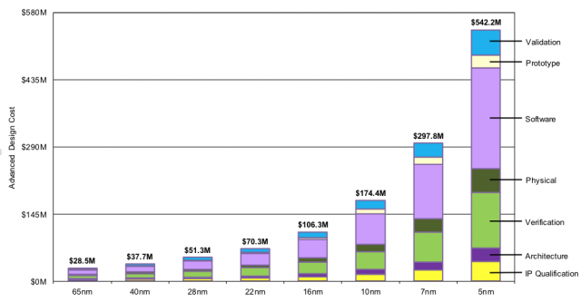
An estimation of Chip Tape Out Costs (Source: IBS)
Fragmenting a chip allows for certain pieces to be re-used multiple times. Reducing costs across the board. Thinking about GPUs, how many years have you seen a PCIe Gen3 be the main interface? Probably for at least the past 4-5 years. That PCIe core is being designed, tested, validated every time a new GPU flavor is released. This increases costs and time to market.
The downsides of course are you can’t take advantage of the newest process node, potentially saving area and power for a respective design. These are obviously design decisions that have to be made based on the application of the chip.
Possible Example Chiplet
Here is a theoretical chiplet idea. Let’s break down a typical SoC into large blocks. We would potentially have the following:
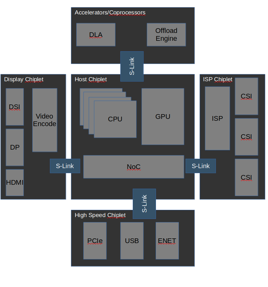
Example SoC built using chiplets
CPU/GPU - The cool things that everyone likes to talk about
Camera - Camera interfaces for mobile and image signal processor(s)
Display - encode/display engines and the various display interfaces
High Speed Connectivity - PCIe, USB, Ethernet and other protocols we use to talk with the outside world
Accelerators and Coprocessors
Looking at this hypothetical SoC, we easily have 12+ block IPs (there are way more in reality). How does Jim Bob’s ASIC team create this SoC? Short answer, they don’t. They can’t even. There are just too many IPs to secure, integration, testing, etc. But if we break it down into chiplets, we now have something that’s more manageable. We can even see how various SKUs can be created without respinning silicon. Let’s say this is a mobile SoC and we have 3 CPU/GPU flavors for low/mid/high tier devices. We want to keep the same cameras, display, and connectivity. We can change out our “Host Chiplet” in this case while maintaining the other display, camera, and high speed chiplets the same. We are not required to re-test the peripherial chiplets, the software remains the same. Do we have a case where we want different high speed connectivity? Replace the chiplet. No display engine because there is a dedicate GPU in the system off-chip? Don’t include the display chiplet.
S-Link allows these chiplets to connect with a simple, open protocol. The data across can be optimized based on the application (memory, pixel data, etc.).
The Future of Hardware Design (?)
There are multiple facets of semiconductors that I believe will contribute to a change in how the industry works.
If we take a step back for a second and look at how things have changed in various other industries. I like to look at YouTube as an example, not YouTube itself, but the individual creators. 50 years ago there were only a handful of channels (I mean, that’s what my parents told me). Now you can go on a website and watch videos that random people created. Last stat I heard was there was something like 400hours of content uploaded every minute to YouTube (going from memory here). Chances are good, that the majority is just garbage, but there is a ton of content that is good, in fact great. I don’t speak for the entire world, but I’m amazed that I get more enjoyment out of a person who creates content on YouTube, in their spare time than cable networks with mulit-million dollar budgets.
This, to me, is an indication of a movement away from large entities towards a more intimate relationship between a creator and their consumers. I have a feeling that this same behavior will translate into hardware design. One may argue that creating a YouTube video is much easier than creating hardware, and you would be correct, however as there are millions of “YouTubers” there are very few who are widely known and create true great content; and they are the ones that filter to the top. These creators also generally make what they want to, allowing them to prioritize what they feel is important. This also constitutes more fuitful content.
I believe that hardware and software design will somewhat migrate to a creator/consumer model, similar to the above. I don’t believe that large entities and corporations will go away, but we will see a surge is individuals creating and supplying IP. The big players will ultimately use these IPs and/or employ/fund the creators. The ultimate business model is yet to be seen with this type of ecosystem, but I’m going to go with a “we’ll cross that bridge when we get to it” mindset.
Note
Currently (August 2020) S-Link is in it’s infancy stages. I expect many changes along the way. These are expected and welcomed and every effort will be made to make changes with grace as to not effect end-users.
Note
“chips” and “chiplets” will be used interchangably throughout the documentation. Just know it’s meant as from one piece of silicon to another.