Integration
Parameters
Name |
Acceptable Values |
Description |
|---|---|---|
NUM_TX_LANES |
1/2/4 |
Maximum number of TX lanes supported by S-Link |
NUM_RX_LANES |
1/2/4 |
Maximum number of RX lanes supported by S-Link |
PHY_DATA_WIDTH |
8 |
Data width of phy data for TX/RX |
TX_APP_DATA_WIDTH |
N * NUM_TX * PHY_DATA_WIDTH
|
Data width of the tx_app_data signals. This must
be a multiple of the PHY_DATA_WIDTH * maximum number
of lanes. N is required to be a factor of 2.
|
RX_APP_DATA_WIDTH |
N * NUM_RX * PHY_DATA_WIDTH
|
Data width of the rx_app_data signals. This must
be a multiple of the PHY_DATA_WIDTH * maximum number
of lanes. N is required to be a factor of 2.
|
DESKEW_FIFO_DEPTH |
4 |
Number of deskew FIFO entries for RX. |
LTSSM_REGISTER_TXDATA |
0/1 |
Adds optional pipeline state in LTSSM. Useful for FPGA,
slower proceses, or higher clock frequencies.
|
INCLUDE_BIST |
0/1 |
1 - Includes the BIST logic. 0 - BIST logic removed |
The RTL is designed such that unused logic is removed based on the parameter settings. e.g. If NUM_TX_LANES == 2 then the logic
for 4+ lanes in the TX path is excluded from the design.
Note
Support for 16/32/64/128 Lanes is coming soon
Support for 32bit phy data widths is coming soon
Currently DESKEW_FIFO_DEPTH should be kept at 4. Future support for upto 16 entries is coming.
Ports
Port Name |
Direction |
Width |
Description |
|---|---|---|---|
DFT |
|||
core_scan_clk |
input |
1 |
Clock for DFT Scan mode |
core_scan_mode |
input |
1 |
DFT Scan mode enable (assertion of this signal will force respective analog signals to a known state) |
core_scan_asyncrst_ctrl |
input |
1 |
DFT Scan mode reset control |
APB |
|||
apb_clk |
input |
1 |
APB Clock |
apb_reset |
input |
1 |
APB Reset (active high) |
apb_paddr |
input |
[7:0] |
APB Address |
apb_pwrite |
input |
1 |
APB pwrite |
apb_psel |
input |
1 |
APB psel |
apb_penable |
input |
1 |
APB penable |
apb_pwdata |
input |
[31:0] |
APB pwdata |
apb_prdata |
output |
[31:0] |
APB prdata |
apb_pready |
output |
1 |
APB pready |
apb_pslverr |
output |
1 |
APB pslverr |
Application Side Signals |
|||
link_clk |
output |
1 |
Link clock to be used by the application layer (this is provided by the PHY and is the refclk
during low power states or when the phy clock is not available)
|
link_reset |
output |
1 |
Link reset synchronized to the link_clk |
tx_sop |
input |
1 |
Application TX Start of Packet |
tx_data_id |
input |
[7:0] |
Application TX Data ID |
tx_word_count |
input |
[15:0] |
Application TX Word Count/Short Packet Payload |
tx_app_data |
input |
[TX_APP_DATA_WIDTH-1:0] |
Applicaiton TX data |
tx_advance |
output |
1 |
Application TX advance to next data block or packet. Indicates that the current application data has been
accepted and the next block of data can be presented.
|
rx_sop |
output |
1 |
Application RX Start of Packet |
rx_data_id |
output |
[7:0] |
Application RX Data ID |
rx_word_count |
output |
[15:0] |
Application RX Word Count/Short Packet Payload |
rx_app_data |
output |
[RX_APP_DATA_WIDTH-1:0] |
Application RX data |
rx_valid |
output |
1 |
Application RX data is valid for this cycle |
rx_crc_corrupted |
output |
1 |
Indicates that the received CRC did not match the calculated value. Can be used by the application layer
to discard the data.
|
p1_req |
input |
1 |
Request S-Link to enter P1 state |
p2_req |
input |
1 |
Request S-Link to enter P2 state |
p3_req |
input |
1 |
Request S-Link to enter P3 state |
in_px_state |
output |
1 |
Indicates the link is in P1/2/3 state |
in_reset_state |
output |
1 |
Indicates the link is in the RESET state |
interrupt |
output |
1 |
Interrupt status |
Phy Signals |
|||
slink_gpio_reset_n_oen |
output |
1 |
Output enable for S-Link Reset sideband. 1 - sideband reset should be driven low. 0 - sideband reset
should be not driven
|
slink_gpio_reset_n |
input |
1 |
S-Link reset sideband value (if this side is not driving, should be value from other side) |
slink_gpio_wake_n_oen |
output |
1 |
Output enable for S-Link wake sideband. 1 - sideband wake should be driven low. 0 - sideband wake
should be not driven
|
slink_gpio_wake_n |
input |
1 |
S-Link wake sideband value (if this side is not driving, should be value from other side) |
refclk |
input |
1 |
Low Speed always free running refclk |
phy_clk |
input |
1 |
High speed PHY clock synchronous with the TX/RX data |
phy_clk_en |
output |
1 |
Enable the PHY CLK logic |
phy_clk_idle |
output |
1 |
1 - PHY CLK should disable clock transmitter/receiver. 0 - Clock should be transmitted/received if phy_clk_en |
phy_clk_ready |
input |
1 |
PHY CLK is up and transmitting/receiving the clock |
phy_tx_en |
output |
[NUM_TX_LANES-1:0] |
Enable TX for data transmission. |
phy_tx_ready |
input |
[NUM_TX_LANES-1:0] |
TX is enabled and ready for data transmission |
phy_tx_dirdy |
input |
[NUM_TX_LANES-1:0] |
TX is not ready to accept data this cycle. Used for PHYs that may need to backpressure data
CURRENTLY UNUSED
|
phy_tx_data |
output |
[(NUM_TX_LANES*
PHY_DATA_WIDTH)-1:0]
|
TX data |
phy_rx_en |
output |
[NUM_RX_LANES-1:0] |
Enable RX for data reception |
phy_rx_clk |
input |
[NUM_RX_LANES-1:0] |
RX clock for each lane. If each RX clock is synchronous to phy_clk, tie phy_clk to these |
phy_rx_ready |
input |
[NUM_RX_LANES-1:0] |
RX is enabled and ready for data reception |
phy_rx_valid |
input |
[NUM_RX_LANES-1:0] |
RX is receiving data and has acquired byte lock |
phy_rx_dordy |
input |
[NUM_RX_LANES-1:0] |
RX data is valid this cycle
CURRENTLY UNUSED
|
phy_rx_align |
output |
[NUM_RX_LANES-1:0] |
Indicates RX is looking for block alignment. Could be used by the RX to enable CDR or other logic. |
phy_rx_data |
input |
[(NUM_RX_LANES*
PHY_DATA_WIDTH)-1:0]
|
RX data |
Application Layer Signaling
An application layer would communicate with S-Link via the application side signals. The app layer would build a conceptual “packet” that is to
be sent, however the app layer isn’t responsible for figuring out how to stripe across lanes, perform error checking, etc. That is the job
of S-Link. The app layer would tell S-Link a new packet is ready to be sent by asserting tx_sop along with a valid tx_data_id, tx_word_count, and
tx_app_data (if sending a long packet). The app layer would hold these signals until tx_advance is seen. tx_advance indicates that the S-Link link layer has
sent the current data and is ready for the next cycle of application data.
Long Packet Example
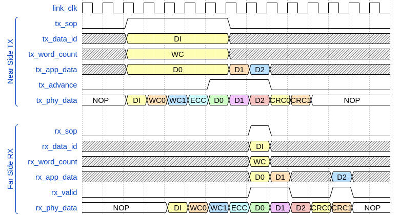
A long packet would supply a Data ID, Word Count, and Application Data and assert tx_sop. S-Link would begin to send the Data Id, Word Count, and ECC (long packet header).
tx_advance is asserted for each cycle when new data is ready to be recieved.
On the other S-Link, the RX would begin to see a new packet coming in. Once the packet header and application data has been seen it will assert rx_sop and rx_valid. rx_valid
will then assert everytime that the complete APP_DATA_WIDTH bits have been seen or until the end of the application data (for example if you send a word count of three (3)
with an APP_DATA_WIDTH of 32, the rx_valid would assert with rx_sop and the MSB ([31:24]) would be invalid.
In the example above, if we assume a one lane S-Link at 8bits we can see how each byte is transmitted to/from the PHY and application layer.
Warning
The application layer must always present valid data after the tx_sop assertion until all bytes are sent based on the word count value. e.g. If word_count equals 12, all 12 bytes need
to be available to S-Link. If the APP_DATA_WIDTH is 32bits, S-Link would set tx_advance 3 times (3 cycles x 4 bytes / cycle = 12 bytes total).
Short Packet Example

A short packet would supply the Data Id and Payload. Application data is ignored. The same tx_sop and tx_advance handshake applies as with the long packet,
however after the tx_advance asserts the application layer can start sending another packet.
On the RX side S-Link will assert rx_sop and rx_valid after the complete packet has been seen.